English
 English
 Español
 Português
 русский
 français
 日本語
日本語 Deutsch
 Tiếng Việt
 Italiano
 Nederlands
 ไทย
ไทย Polski
 한국어
한국어 Svenska
 magyar
 Malay
Malay বাংলা
বাংলা Dansk
Dansk Suomi
Suomi हिन्दी
 Pilipino
 Türk
Türk Gaeilge
 عربى
عربى Indonesia
 norsk
norsk Burmese
 български
 ລາວ
ລາວ Latine
 Қазақ
Қазақ Euskal
 Azərbaycan
 slovenský
 Македонски
 Română
 Slovenski
 Српски
 Afrikaans
 Беларус
 Hrvatski
 Монгол хэл
 Zulu
Zulu Somali
 O'zbek
 Hawaiian

 Consume Grade Phototransistor Optocoupler OR-3H7-EN-V13
 Consume Grade Phototransistor Optocoupler OR-3H7-4-EN-V3
 Consume Grade Phototransistor Optocoupler OR-3H4-EN-V12
 Consume Grade Phototransistor Optocoupler OR-3H4-4-EN-V3
 Consume Grade Phototransistor Optocoupler ORPC-817-S-(SJ)
- Consume Grade Phototransistor Optocoupler ORPC-817-S-(SJ)-EN-V0
- All new products


Consume Grade Phototransistor Optocoupler OR-3H7-EN-V13
The OR-3H7-4 series device contains four infrared led and four photo transistor detector. They are encapsulated in a 16-pin SOP, free of halogens and Sb2O3
Product Description
Optocoupler 3H7
Features
(1) 4N2X series: 4N25, 4N26, 4N27, 4N28;4N3X series: 4N35, 4N36, 4N37, 4N38
-
High isolation voltage between input and output (Viso=5000 V rms)
-
Creepage distance >7.62 mm
-
Operating temperature up to +115°C
-
Compact dual-in-line package
-
ESD pass HBM 8000V/MM 2000V
-
Safety approval
UL approved(No.E323844)
VDE approved(No.40029733)
CQC approved (No.CQC19001231480 )
-
In compliance with RoHS, REACH standards.
-
MSL Class Ⅰ
Instructions
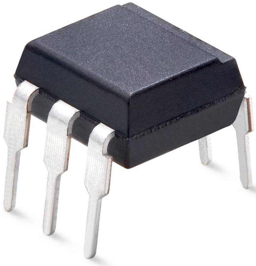
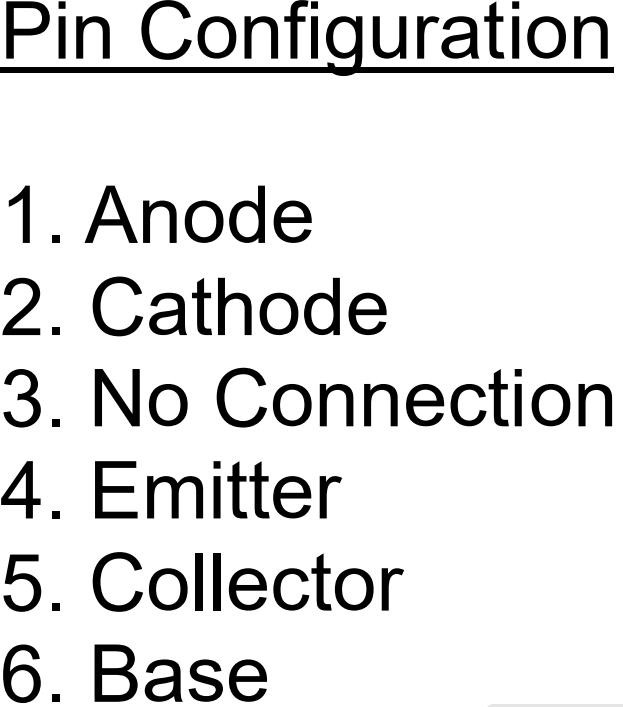
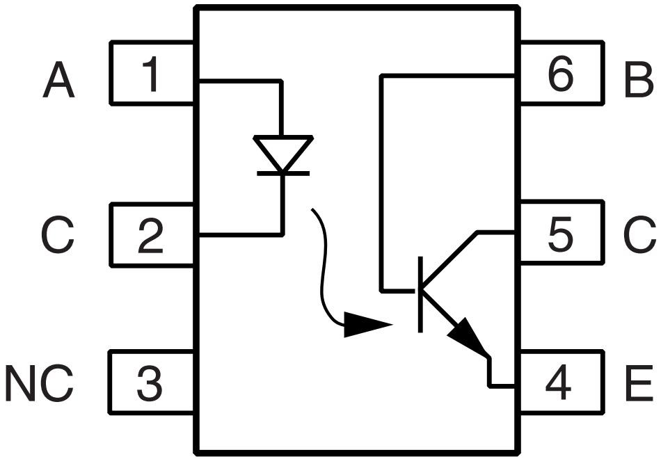
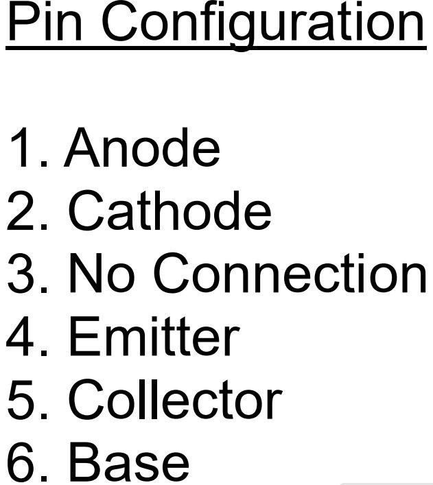
The 4N2X, 4N3X, series of devices each consist of an infrared emitting diode
optically coupled to a photo transistor.They are packaged in a 6-pin DIP package and available in wide-lead spacing and SMD option.
Application Range
-
Power supply regulators
-
Digital logic inputs
-
Microprocessor inputs
Functional Diagram

Max Absolute rated Value (Normal Temperature=25℃)
|
Parameter |
Symbol |
Rated Value |
Unit |
|
|
Input |
Forward Current |
IF |
60 |
mA |
|
Junction Temperature |
TJ |
125 |
℃ |
|
|
Reverse Voltage |
VR |
6 |
V |
|
|
Power dissipation (T A = 25°C) Derating factor (above 100°C) |
PD |
100 |
mW |
|
|
3.8 |
mW/°C |
|||
|
Output |
Collector-emitter Voltage |
VCEO |
80 |
V |
|
Collector-Base voltage |
VCBO |
80 |
||
|
Emitter-Collector voltage |
VECO |
7 |
||
|
Emitter-Base voltage |
VEBO |
7 |
||
|
Power dissipation (T A = 25°C) Derating factor (above 100°C) |
PC |
150 |
mW |
|
|
9.0 |
mW/°C |
|||
|
Total Consume Power |
Ptot |
200 |
mW |
|
|
*1 Insulation Voltage |
Viso |
5000 |
Vrms |
|
|
Working Temperature |
Topr |
-55 to + 115 |
℃ |
|
|
Deposit Temperature |
TSTG |
-55 to + 150 |
||
|
*2 Soldering Temperature |
TSOL |
260 |
||
*1. AC Test, 1 minute, humidity = 40~60% Insulation test method as below:
- Short circuit both terminals of photocoupler.
- No Current when testing insulation voltage.
- Adding sine wave voltage when testing
*2. soldering time is 10 seconds.
Opto-electronic Characteristics
|
Parameter |
Symbol |
Min |
Typ.* |
Max |
Unit |
Condition |
||
|
Input |
Forward Voltage |
VF |
--- |
1.2 |
1.5 |
V |
IF=10mA |
|
|
Reverse Current |
IR |
--- |
--- |
10 |
μA |
VR=6V |
||
|
Collector capacitance |
Cin |
--- |
30 |
--- |
pF |
V=0, f=1MHz |
||
|
Output |
Collector-Base dark current |
ICBO |
--- |
--- |
20 |
nA |
VCB=10V |
|
|
Collector to emitter Current |
4N2X |
ICEO |
--- |
--- |
50 |
nA |
VCE=10V, IF=0mA |
|
|
4N3X |
--- |
--- |
50 |
VCE= 60V, IF=0mA |
||||
|
Collector-Emitter attenuation Voltage |
BVCEO |
80 |
--- |
--- |
V |
IC=1mA |
||
|
Collector-Base breakdown voltage |
BVCBO |
80 |
IC=0.1mA |
|||||
|
Emitter-Collector attenuation Voltage |
BVECO |
7 |
--- |
--- |
V |
IE=0.1mA |
||
|
Emitter-Base breakdown voltage |
BVEBO |
7 |
IE=0.1mA |
|||||
|
Transforming Characteristics |
Current Transfer ratio |
4N35, 4N36,4N37 |
CTR |
100 |
--- |
--- |
% |
IF=10mA VCE=10V |
|
4N25, 4N26,4N38 |
20 |
--- |
--- |
|||||
|
4N27, 4N28 |
10 |
--- |
--- |
|||||
|
Collector and Emitter Saturation Voltage |
4N25, 4N26,4N27, 4N28 |
VCE(sat) |
--- |
--- |
0.5 |
V |
IF=50mA IC=2mA |
|
|
4N35, 4N36,4N37 |
--- |
--- |
0.3 |
IF=10mA, IC=0.5mA |
||||
|
4N38 |
--- |
--- |
1.0 |
IF=20mA, IC=4mA |
||||
|
Isolation resistance |
Riso |
1011 |
--- |
--- |
Ω |
DC500V 40~60%R.H. |
||
|
Floating Capacitance |
Cf |
--- |
0.2 |
--- |
pF |
V=0, f=1MHz |
||
|
Response Time |
tr |
--- |
3 |
10 |
μs |
VCC=10V, IC=10mA RL=100Ω |
||
|
Descend Time |
tf |
--- |
6 |
10 |
μs |
|||
-
Current Conversion Ratio = IC / IF × 100%
Order Information
Part Number
OR-4NXXU-Y-Z
Note
4NXX = Part Number, 4N25,4N26,4N27,4N28,4N35,4N36,4N37 or 4N38.
U = Lead form option (S, M or None)
Y = Tape and reel option (TA,TA1 or none).
Z = ‘V’ code for VDE safety (This options is not necessary).
* VDE Code can be selected.
|
Option |
Description |
Packing quantity |
|
None |
Standard DIP-6 |
66 units per tube |
|
M |
Wide lead bend (0.4 inch spacing) |
66 units per tube |
|
S(TA) |
Surface mount lead form (low profile) + TA tape & reel option |
1000 units per reel |
|
S(TA1) |
Surface mount lead form (low profile) + TA1 tape & reel option |
1000 units per reel |
Naming Rule
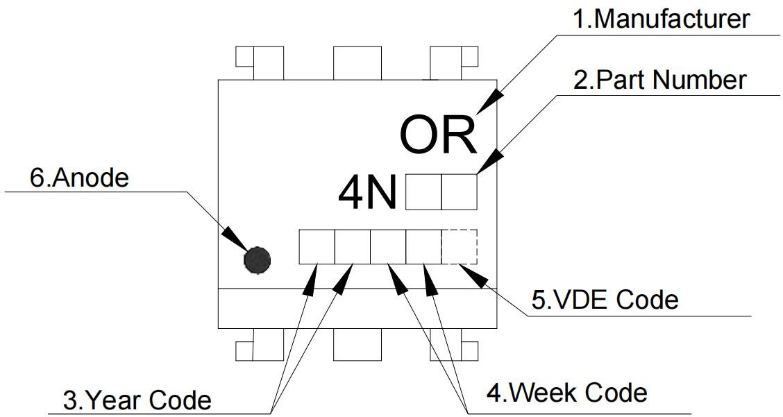
1. Manufacturer : ORIENT.
2. Part Number : 4N25,4N26,4N27,4N28,4N35,4N36,4N37 or 4N38.
-
Year Code
 : '21' means '2021' and so on.
 -
Week Code
: 01 means the first week, 02 means the second week and so on. -
VDE Code
 . (Optional)
 -
Anode.
Outer Dimension
OR-4NXX
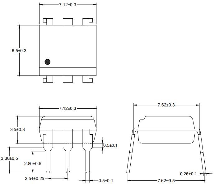
OR-4NXXM
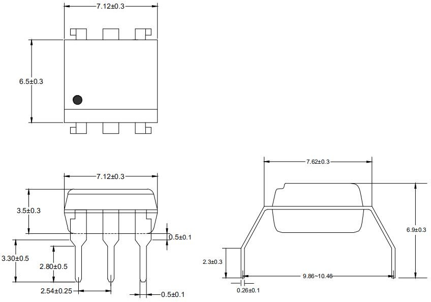
OR-4NXXS
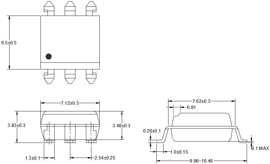
Recommended Foot Print Patterns (Mount Pad)
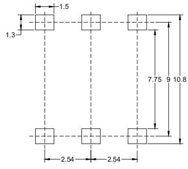
unit:mm
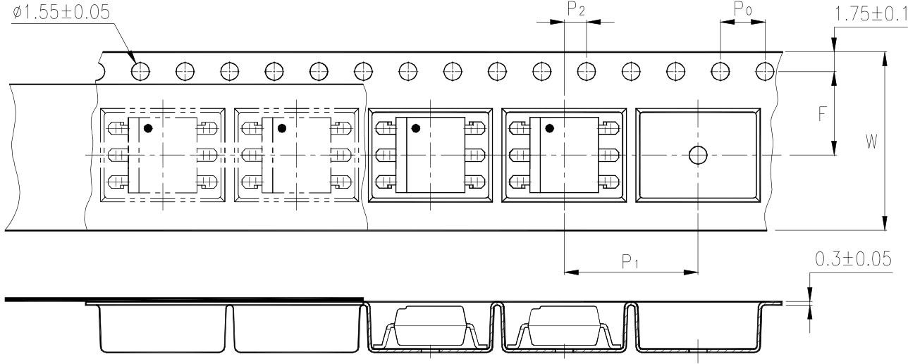
Taping Dimensions
OR-4NXXS-TA
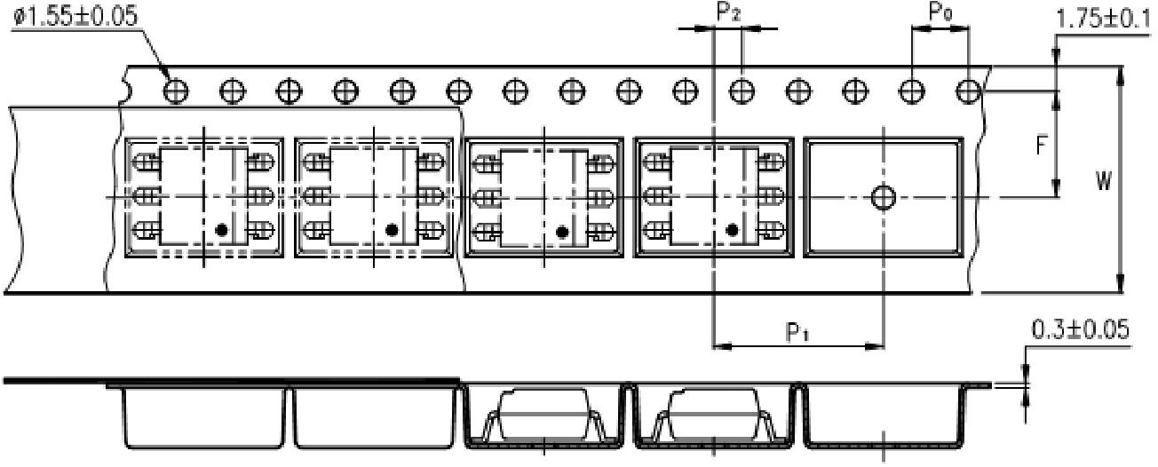
OR-4NXXS-TA1
|
Description |
Symbol |
Dimension in mm(inch) |
|
Tape wide |
W |
16±0.3(0.63) |
|
Pitch of sprocket holes |
P0 |
4±0.1(0.15) |
|
Distance of compartment |
F |
7.5±0.1(0.295) |
|
P2 |
2±0.1(0.079) |
|
|
Distance of compartment to compartment |
P1 |
12±0.1(0.472) |
|
Package Type |
TA/TA1 |
|
Quantities(pcs) |
1000 |
Package Dimension
DIP/M type
|
Packing Information |
|
|
Packing type |
Tube |
|
Qty per Tube |
66pcs |
|
Small box (Inner) Dimension |
525*128*60mm |
|
Large box (Outer) Dimension |
545*290*335mm |
|
The Amount per Inner Box |
3,300pcs |
|
The Amount per Outer Box |
33,000pcs |
SOP type
|
Packing Information |
|
|
Packing type |
Reel type |
|
Tape Width |
16mm |
|
Qty per Reel |
1,000pcs |
|
Small box (inner) Dimension |
345*345*58.5mm |
|
Large box (Outer) Dimension |
620x360x360mm |
|
Max qty per small box |
2,000pcs |
|
Max qty per large box |
20,000pcs |
Packing Label Sample
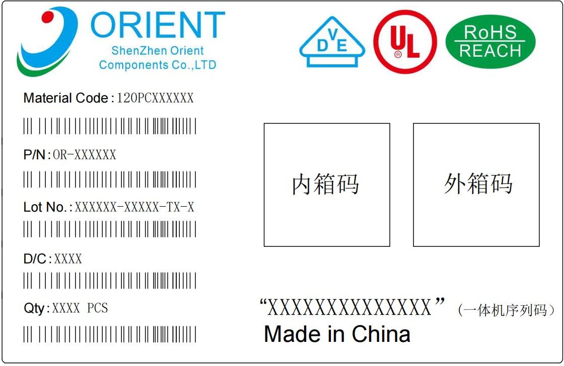
Note:
-
Material Code :Product ID.
-
P/N :Contents with "Order Information" in the specification.
-
Lot No. :Product data.
-
D/C :Product weeks.
-
Quantity :Packaging quantity.
Reliability Test
-
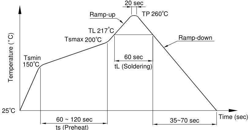
Temperature Profile Of Soldering
(1) IR Reflow soldering (JEDEC-STD-020C compliant)
One time soldering reflow is recommended within the condition of temperature and time profile shown below. Do not solder more than three times.
|
Profile item |
Conditions |
|
Preheat
- Time (min to max) (ts) |
150˚C 200˚C 90±30 sec |
|
Soldering zone - Temperature (TL ) - Time (t L ) |
217˚C 60 sec |
|
Peak Temperature |
260˚C |
|
Peak Temperature time |
20 sec |
|
Ramp-up rate |
3˚C / sec max. |
|
Ramp-down rate from peak temperature |
3~6˚C / sec |
|
Reflow times |
≤3 |
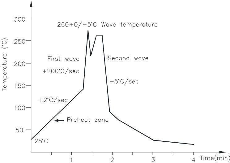
(2) Wave soldering (JEDEC22A111 compliant)
One time soldering is recommended within the condition of temperature.
|
Temperature Time |
260+0/-5˚C 10 sec |
|
Preheat temperature Preheat time |
25 to 140˚C 30 to 80 sec |
(3) Hand soldering by soldering iron
Allow single lead soldering in every single process. One time soldering is recommended.
Temperature
380+0/-5˚C
Time
3 sec max
Characteristics Curve


")
