English
 English
 Español
 Português
 русский
 français
 日本語
日本語 Deutsch
 Tiếng Việt
 Italiano
 Nederlands
 ไทย
ไทย Polski
 한국어
한국어 Svenska
 magyar
 Malay
Malay বাংলা
বাংলা Dansk
Dansk Suomi
Suomi हिन्दी
 Pilipino
 Türk
Türk Gaeilge
 عربى
عربى Indonesia
 norsk
norsk Burmese
 български
 ລາວ
ລາວ Latine
 Қазақ
Қазақ Euskal
 Azərbaycan
 slovenský
 Македонски
 Română
 Slovenski
 Српски
 Afrikaans
 Беларус
 Hrvatski
 Монгол хэл
 Zulu
Zulu Somali
 O'zbek
 Hawaiian

 Consume Grade Phototransistor Optocoupler OR-3H7-EN-V13
 Consume Grade Phototransistor Optocoupler OR-3H7-4-EN-V3
 Consume Grade Phototransistor Optocoupler OR-3H4-EN-V12
 Consume Grade Phototransistor Optocoupler OR-3H4-4-EN-V3
 Consume Grade Phototransistor Optocoupler ORPC-817-S-(SJ)
- Consume Grade Phototransistor Optocoupler ORPC-817-S-(SJ)-EN-V0
- All new products


Darlington Optocoupler OR-4NXX_OR-TIL113(Darlington)-EN-V3
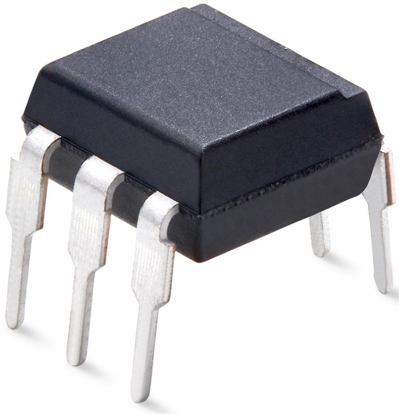
The TIL113, 4NXX series of devices each consist of an infrared emitting diode optically coupled to a darlington detector.They are packaged in a 6-pin DIP package and available in wide-lead spacing and SMD option.
Product Description
Darlington Optocoupler
Features
(1) 4NXX series: 4N29, 4N30, 4N31, 4N32, 4N33 TIL113 series: TIL113.
(2) High isolation voltage between input and output (Viso=5000 V rms)
(3) Creepage distance >7.62 mm
(4) Operating temperature up to +115°C
(5) Compact dual-in-line package
(6) Safety approval
UL approved(No.E323844)
VDE approved(No.40029733)
CQC approved (No.CQC19001231480 )
(7) In compliance with RoHS, REACH standards.
(8) MSL Class Ⅰ
Instructions
The TIL113, 4NXX series of devices each consist of an infrared emitting diode optically coupled to a darlington detector.They are packaged in a 6-pin DIP package and available in wide-lead spacing and SMD option.
Application Range
-
Low power logic circuits
-
Telecommunications equipment
-
Portable electronics
-
Interfacing coupling systems of different potentials and impedances
Max Absolute rated Value (Normal Temperature=25℃)
|
Parameter |
Symbol |
Rated Value |
Unit |
|
|
Input |
Forward Current |
IF |
60 |
mA |
|
Junction Temperature |
TJ |
125 |
℃ |
|
|
Reverse Voltage |
VR |
6 |
V |
|
|
Power dissipation (TA = 25°C) Derating factor (above 100°C) |
PD |
120 |
mW |
|
|
3.8 |
mW/°C |
|||
|
Output |
Collector-emitter Voltage |
VCEO |
80 |
V |
|
Collector-Base voltage |
VCBO |
80 |
||
|
Emitter-Collector voltage |
VECO |
7 |
||
|
Emitter-Base voltage |
VEBO |
7 |
||
|
Power dissipation (T A = 25°C) Derating factor (above 100°C) |
PC |
150 |
mW |
|
|
6.5 |
mW/°C |
|||
|
Total Consume Power |
Ptot |
200 |
mW |
|
|
*1 Insulation Voltage |
Viso |
5000 |
Vrms |
|
|
Working Temperature |
Topr |
-55 to + 115 |
℃ |
|
|
Deposit Temperature |
TSTG |
-55 to + 150 |
||
|
*2 Soldering Temperature |
TSOL |
260 |
||
*1. AC Test, 1 minute, humidity = 40~60% Insulation test method as below:
-
-
Short circuit both terminals of photocoupler.
-
Current when testing insulation voltage.
-
Adding sine wave voltage when testing
-
*2. soldering time is 10 seconds.
Opto-electronic Characteristics
|
Parameter |
Symbol |
Min |
Typ.* |
Max |
Unit |
Condition |
||
|
Input |
Forward Voltage |
VF |
--- |
1.2 |
1.5 |
V |
IF=10mA |
|
|
Reverse Current |
IR |
--- |
--- |
10 |
μA |
VR=6V |
||
|
Collector capacitance |
Cin |
--- |
50 |
--- |
pF |
V=0, f=1MHz |
||
|
Output |
Collector-Base dark Current |
ICBO |
--- |
--- |
20 |
nA |
VCB=10V |
|
|
Collector to emitter Current |
ICEO |
--- |
--- |
100 |
nA |
VCE=10V, IF=0mA |
||
|
Collector-Emitter attenuation Voltage |
BVCEO |
55 |
--- |
--- |
V |
IC=1mA |
||
|
Collector-Base breakdown Voltage |
BVCBO |
55 |
--- |
--- |
V |
IC=0.1mA |
||
|
Emitter-Collector attenuation Voltage |
BVECO |
7 |
--- |
--- |
V |
IE=0.1mA |
||
|
TransformingCharacteristic s |
Current Transfer ratio |
4N32,4N33 |
CTR |
500 |
--- |
--- |
% |
IF=10mA VCE=10V |
|
4N29,4N30 |
100 |
--- |
--- |
|||||
|
4N31 |
50 |
--- |
--- |
|||||
|
TIL113 |
300 |
--- |
--- |
IF=10mAVCE=1V |
||||
|
Collector and Emitter Saturation Voltage |
4N29, 4N30, 4N32,4N33 |
VCE(sat) |
--- |
--- |
1.0 |
V |
IF=8mA IC=2mA |
|
|
4N31,TIL113 |
--- |
--- |
1.2 |
IF=8mA, IC=2mA |
||||
|
Isolation Resistance |
Riso |
1011 |
--- |
--- |
Ω |
DC500V 40~60%R.H. |
||
|
Input-output Capacitance |
CIO |
--- |
0.8 |
--- |
pF |
VIO=0, f=1MHz |
||
|
Response Time |
tr |
--- |
3 |
10 |
μs |
VCC=10V, IC=10mARL=100Ω |
||
|
Descend Time |
tf |
--- |
6 |
10 |
μs |
|||
-
Current Conversion Ratio = IC / IF × 100%
Order Information
Part Number
OR-4NXXY-Z-W
or OR-TIL113Y-Z-W
Note
4NXX = Part Number (4N29,4N30,4N31,4N32 or 4N33)
TIL113= Part Number
Y = Lead form option (S, M or None)
Z = Tape and reel option (TA,TA1 or none).
W= ‘V’code for VDE safety (This options is not necessary).
*VDE Code can bes elected.
|
Option |
Description |
Packing quantity |
|
None |
Standard DIP-6 |
66 units per tube |
|
M |
Wide lead bend (0.4 inch spacing) |
66 units per tube |
|
S(TA) |
Surface mount lead form (low profile) + TA tape & reel option |
1000 units per reel |
|
S(TA1) |
Surface mount lead form (low profile) + TA1 tape & reel option |
1000 units per reel |


